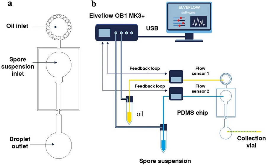
A microfluidic chip was created by soft-lithography technique. The chip was designed under the software AutoCAD 2018 (Autodesk, Inc) (Fig. 5a) and printed on a photomask by CAD/Art (CAD/Art Services, Inc, USA). A mold of SU8-2050 negative photoresist (MicroChem Corp, USA.) was prepared on a silicon wafer (Siltronix) by UV exposure (UV-KUB, Klo��, France) through a photomask and subsequent development (SU-8 developer; MicroChem Corp.). A curing agent was added to PDMS base (Sylgard 184 elastomer kit; Dow Corning Corp.) to a final concentration of 10% (w/w), mixed, and poured onto the mold. After degassing under vacuum, the mold was incubated for five hours at 65 ��C. PDMS was then peeled off and inlets and outlets were punched with biopsy punch (Ø 0.75 mm; Eloise, France). The structured side of the PDMS was bound to a glass microscope slide (Corning) by exposing both parts to an oxygen plasma (Harrick Plasma) equipped with Equinox (BlackHole Lab, France). The microfluidic chips were treated with Aquapel (Autoserv, Germany) followed by HFE-7500 oil (Novec7500, 3 M). A spore suspension of a precise concentration (2 �� 104 spores mL−1) according to Poisson Law54 (�� = 0.01) was prepared from 7�C8 days old sporulating cultures of A. alternata in half strength PDB (Dutscher, France). The spore suspension was filtered using nylon filtration tissue NITEX, mesh opening 50 ��m (Dutscher, France) and 0.1% Tween 20 (Sigma, Aldrich) was added. The reservoirs were filled with spore suspension and HFE-7500 fluorinated oil diluted with 1% surfactant (Emulseo, France) and connected to the microfluidic chip by OD 1/32�� tubing. The reservoirs were connected to the OB1 pressure controller (Elveflow, France) outlet to control flow rates through the ESI software (Fig. 5b). The droplet size for single spore encapsulation was optimized by applying different pressures to accommodate single spore.
PDMS����оƬͨ����������̼�������������Ҫ��������Ҫ���裺
1���ӹ�SU8-2050ģ��
2����SU8ģ���ϸ��ƴ��й�����PDMSƬ��Ȼ���PDMSƬ�������ز�Ƭ������������ϴ������������һ��
3������Aquapel����Fluo-ST2��ˮ�Լ�����PDMSоƬ�������γ���ˮ���ʣ�����ǿ�Ͱ�ˮ���͵�Һ�β���������ֹҺ���ںϺ��žۡ�
4������ѡ���ô���FluoSurf������Լ������������7500ע�뵽PDMSоƬ�����ڣ��Խ��ͷ�ɢ������������PDMS�����IJ���ϡ�
�����ݽ�ѡ������
Droplet-based microfluidics platform for antifungal analysis against filamentous fungi
Iftikhar, S., Vigne, A. & Sepulveda-Diaz, J.E. Droplet-based microfluidics platform for antifungal analysis against filamentous fungi. Sci Rep 11, 22998 (2021). https://doi.org/10.1038/s41598-021-02350-8


